Tuesday, December 22, 2015

Internet of Things (IOT) Dreams Facing Three Constraints


In the middle of a wonderful dream that is offered through the application of Internet of Things (IOT), a number of challenges have been mapped in the Internet of Things World Forum 2015 held at Dubai World Trade Center, Dubai, United Arab Emirates in 6-8 Dec 2015.

Cisco noted, there are three challenges that make the development of IOT has not been too rapidly growth until now. The three constraints of IOT applications are interoperability, security and innovation.

Interoperability is the ability of different platforms to connect each others. Cisco with Dell, Princeton University, ARM, Intel and Microsoft are supporting the development of IOT form OpenFog Consortium to overcome this challenge.

Secuirty issues are related to how to make big data analaytics better, install sensors, and cyber security. Cisco made a protection package which consists of the network itself, and to install more sensors in order to close the security gap that may arise due to the increasing number of devices connected to the internet.

An active network can detect danger, enforcing rules and regulations accelerate, and accelerate the settlement of security issues found.

The third is innovation, about dreaming, thinking what else is likely to be realized, bold imagination. In terms of encouraging innovation, one way through the IOT World Forum 2015 held in Dubai World Trade Center.

Tuesday, October 14, 2014

VHDL Codes for Train Controller using State Machine

ASM Train Controller VHDL
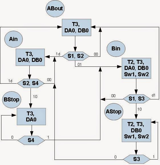
Fig 1. ASM Diagram of Electric Train Controller
This posting will discuss a working example of a train controller using state machine. In this controller, two trains run counterclockwise at various speeds and avoid collisions. One train (A) runs on the outer track and the other (B) runs on the inner track. Only one train at a time is allowed to occupy the common track.

An ASM chart and State Machine diagram shown in figure 1 (above) and figure 2 contain the same information and describe algorithm of the train controller. In the ASM chart, state names, ABout, Ain, Bin, Bstop, Astop indicate the active and possible states. The rectangles contain the active (High) outputs for the given state. Outputs not listed are inactive (Low). The diamond shapes in the ASM chart indicate where the state machine tests the condition of the inputs (S1, S2, etc.). When two signals are shown in a diamond, they are both tested at the same time for the indicated values.

A state machine classic bubble diagram is shown in Figure 2 below. In the same names "in" and "out" refers to the state of track 2, the track that is common to both loops.


Description of The State Machine for Electric Train Controller
State machine Train Controller VHDL
Fig. 2  State Machine Diagram of Electric Train Controller

Tuesday, September 9, 2014

CPLD Development Board


CPLD development board image
Fig.1 Top & bottom sides of Xilinx CPLD
A CPLD (Complex Programmable Logic Design) is a combination of a fully programmable AND/OR array and a bank of macrocells.The AND/OR array is reprogrammable and can perform a multiple of logic functions. Macrocells are functional blocks that perform combinatorial or sequential logic, and also have the added flexibility for true or complement, along with varied feedback paths. 

Traditionally, CPLDs have used analog sense amplifiers to boost the performance of their architectures. CPLDs perform a variety of useful functions in systems design due to their unique capabilities and as the market leader in programmable logic solutions, Xilinx provides a total solution to a designer's CPLD needs. (http://www.xilinx.com/cpld).

A lot of logic devices are hosed in a CPLD and those connections can be specified by the program (software). As an example, 7400 IC consists of 4 circuits of 2 input NAND gates that are housed inside. Another example is 7404 IC that consists of 6 circuits of inverter inside. In case of CPLD, it has wiring among the logic in the IC, so that the writing on the printed board can be made little. Detail descriptions of this could be shown in the following figure.

CPLD development board

Fig.2 Logic gates and connections in the CPLD


CPLD has a limited capacity and the number of pins compared to FPGA. It is not better to use it in excessive expectations, this means if you has a large or complex digital circuit design the use of FPGA is suggested. The table below describes CPLD specifications of the part of the XC9500 series from Xilinx.Inc.

Parts Name Number of PinsSpecifications
XC9536-15PC44C 44pin PLCC2FB/36macrocells/800gates
XC9572-15PC44C 44pin PLCC4FB/72macrocells/1600gates
XC9572-15PC84C 84pin PLCC4FB/72macrocells/1600gates
XC95108-15PC84C 84pin PLCC6FB/108macrocells/2400gates


The point which CPLD is convenient for is the thing about which it is possible to rewrite many times because it is recording the contents of the circuit to the flash memory. In the XC9500 series, rewriting in about 10,000 times is possible. Since the pins for the rewriting is preparatory, the contents can be rewritten in the condition to have mounted to the actual circuit if wiring is exist. The Figure 3 shows the block diagram of CPLD XC9500 series.

Saturday, July 12, 2014

Hierarchical Design in VHDL

[1] Functions 

Functions are a simple way of encapsulating behavior in a model that can be reused in multiple architectures. Functions can be defined locally to an architecture or more commonly in a package, but in this section the basic approach of defining functions will be described. The simple form of a function is to define a header with the input and output variables as shown below:

      function name (input declarations) return output_type is
           ... variable declarations
      begin
           ... function body
      end

For example, a simple function that takes two input numbers and multiplies them together could be defined as follows:
             
      function mult (a, b: integer) return integer is
      begin
           return a * b;
      end; 

[2] Packages 

Packages are a common single way of disseminating type and function information in the VHDL design community. The basic definition of a package is as follows:

      package name is
           ... package header contents
      end package;
      package body name is
      begin
           ... package body contents
      end package body;

As can be seen, the package consists of two parts, the header and the body. The header is the place where the types and functions are declared, and the package body is where the declarations themselves take place.

For example, a function could be described in the package body and the function is declared in the package header. Take a simple example of a function used to carry out a simple logic function:

      and10 = and(a, b, c, d, e, f, g, h, i, j)

The VHDL function would be something like the following:

      function and10 = and(a,b,c,d,e,f,g,h,i,j: bit) return bit is 
      begin
        return a and b and c and d and e and f and g and h and i and j;
      end;

The resulting package declaration would then use the function in the body and the function header in the package header thus:
   
      package new_functions is 
      function and10 = and(a,b,c,d,e,f,g,h,i,j: bit) return bit;
      end;
      package body new_functions is       
         function and10 = and(a,b,c,d,e,f,g,h,i,j: bit) return bit is;
           begin
              return a and b and c and d and e \ 
                  and f and g and h and i and j;
           end;
      end;


[3] Components

While procedures, functions and packages are useful in including behavioral constructs generally, with VHDL being used in hardware design context, often there is a need to encapsulate design blocks as a separate component that can be included in a design, usually higher in the system hierarchy.

To be continued


[4] Procedures

Procedures are similar to functions, except that they have more flexibility in the parameters, in that the direction can be in.

To be continued

Friday, July 11, 2014

Parallel Execution in FPGA


Parallel-execution-FPGA
Higher-performance, resource-hungry, MAC-intensive DSP algorithms may benefit from implementation within FPGA components. FPGA architectural enhancements, development tool flow advances, speed increases and cost reductions are making implementation within FPGAs increasingly attractive. FPGA technology advances include increased clock speeds, specialized DSP blocks, tool enhancements and an increasing range of intellectual property solutions. Figure above illustrates an example parallel implementation of an FIR filter within an FPGA.

The MAC operational group may be implemented in one of several different configurations within an FPGA. Three popular implementation options for the MAC operational group within an FPGA are listed below.
  • Both the multiplier and the accumulator may be implemented within the logic fabric of the FPGA taking advantage of FPGA structures, such as dedicated high-speed carry chains.
  • The multiplier may be implemented in an optimized multiplier block, avoiding use of FPGA fabric logic with the accumulator implemented within the logic fabric of the FPGA.
  • Both the multiplier and accumulator may be implemented within an advanced multiplier block requiring the use of no FPGA logic.
Figure below illustrates the three different MAC implementation options. Each of these approaches will be heavily dependent on the architecture of the FPGA fabric, the algorithms being implemented, the performance required and the amount of functionality being implemented on the FPGA component. For example, older device families may not support the integrated accumulator function within the DSP block. In this situation, the DSP block is actually just a multiplier. Likewise, if all the DSP blocks have been used for higher-performance algorithms, it may be possible to implement implement an algorithm with no DSP blocks within the FPGA logic fabric. FPGA DSP blocks are generally implemented in either a column or row structure within the FPGA fabric.


To be continued

Saturday, June 14, 2014

Decisions and Loops in VHDL

[1] If- Then - Else
The basic syntax for a simple if statement is as follows:

            signal (condition) then
           ...statements
      end if;

The condition is a Boolean expression, of the form a > b or a = b. Note that the comparison operator for equality is a single =, not to be confused with the double == used in some programming languages. For example, if two signals are equal, then set an output high would be written in VHDL as:

            if (a = b) then
            out1 <= `1';
      end if;
If the decision needs to have both the if and else options, then the statement is extended as follows:
      
      if (condition) then
           ...statements
      else
           ...statements     
      end if;
So in the previous example, we could add the else statements as follows: 

            if (a = b) then
           out1 <= `1';
      else
           out1 <= `0';     
      end if;

And finally, multiple if conditions can be implemented using the general form:
      
      if (condition1) then
           ...statements
      elseif (condition2)
           ...statements 
           ...more elsif conditions & statements     
      else
           ...statements
      end if;

With an example: 
      
      if (a > 10) then
           out1 <= `1';
      elseif (a > 5) then
           out1 <= `0';    
      else
           out1 <= `1';
      end if;


[2] Case
IF statement is relatively simple to define multiple conditions, but it becomes a little cumbersome, and so the case statement offers a simple approach to branching, without having to use Boolean conditions in every case. This is especially useful for defining state diagrams or for specific transitions between states using enumerated types. An example of a case statement is:

      case testvariable is
         when 1 =>
            out1 <= '1';
     
         when 2 =>
            out2 <= '1';

         when 3 =>
            out3 <= '1';
      end case;

Wednesday, June 11, 2014

Basic Variable Types and Operators in VHDL

This section will discuss on Constants, Signals, Variables, Boolean Operators, Arithmetic Operators, Comparison Operators, Shifting Functions and Concatenation in VHDL.

[1]. Constants
Element type of constants will be used when a value needs to be static throughout a simulation. Constants often used to initialize parameters or to set fixed register values for comparison. A constant can be declared for any defined type in VHDL with examples as follows;

     constant a : integer := 1;
     constant b : real := 0.123;
     constant c : std_logic := `0';    


[2]. Signals
Signals are the link between processes and sequential elements within the processes. Signals are effectively "wires" in the design and connect all the design elements together.
Signals can be assigned immediately or with a time delay, so that an event is scheduled for sometime in the future (after the specified delay). It is also important to recognize that signals are not the same as a set of sequential program code, but are effectively concurrent signals that will not be able to be considered stable until the next time the process is activated.
Examples of signal declaration and assignment are shown below:
     
     signal sig1 : integer := 0;
     signal sig2 : integer := 1;
     sig1 <= 14; 
     sig1 <= sig2; 
     sig1 <= sig2 after 10 ns;  

Monday, March 3, 2014

Process: Basic Functional Unit in VHDL

basic-functional-unit-VHDL
The process in VHDL is the mechanism by which sequential statements can be executed in the correct sequence, and with more than one process, concurrently. Each process consists of a sensitivity list, declarations and statements. The basic process syntax is given below:

     process sensitivity_list is
          ... declaration part
        
     begin
          ... statement part
         
     end process;


The sensitivity list allows a process to be activated when a specific signal changes value, for example a typical usage would be to have a global clock (clk) and reset (rst) signal to control the activity of the process, for example:

     process (clk, rst) is
        
     begin
          ...process statements
         
     end process;


In this example, the process would only be activated when either clk or rst changed value. Another way of encapsulating the same behavior is to use a wait statement in the process so that the process is automatically activated once, and then waits for activity on either signal before running the process again. The same process could then be written as follows:

Wednesday, February 26, 2014

Architecture: Behavioral Modelling in VHDL

behavioral-modelling-VHDL

1. Basic Definition of an Architecture

While the entity describes the interface and parameter aspects of the model, the architecture defines the behavior. There are several types of VHDL architecture and VHDL allows different architectures to be defined for the same entity. This is ideal for developing behavioral, Register Transfer Level RTL and gate Level architectures that can be incorporated into designs and tested using the same test benches.

The basic approach for declaring an architecture could be as follows:
 
     architecture behaviour of test is
         ..architecture declarations
         
      begin
          ..architecture contents

     end architecture behaviour;

Or
          
     architecture behaviour of test is
          ..architecture declarations
      
      begin
          ..architecture contents
        
     end behaviour;

Monday, February 24, 2014

Entity: Interface Model in VHDL

vhdl-structure-interface-model

1. Entity Definition

The entity defines how a design element described in VHDL connects to other VHDL models and also defines the name of the model. The entity also allows the definition of any parameters that are to be passed into the model using hierarchy. Figure beside is overall structure of a VHDL module. 

The basic template for an entity is as follows:

     entity <name> is 

          ...

     entity <name>;
  
If the entity has the name "test", then the entity template could be either: 
     entity test is
     end entity test

or:
      entity test is
     end test;


2. Ports

The method of connecting entities together is using PORTS. These are defined in the entity using the following method:
      port(
      ... list of port declarations...
      );

The port declaration defines the type of connection and direction where appropriate. For example, the port declaration for an input bit called in1 would be as follows:
      in1 : in bit;

Thursday, February 20, 2014

FPGA DSP Design Considerations

FPGA-DSP-considerations
Some of the FPGA design issues that are important to signal processing algorithm implementation are discussed below. These design factors must be carefully implemented in order to achieve the highest levels of performance and fastest design implementation.
  • Synchronous design implementation
  • Modular project structure
  • Clock boundary transitions
  • Clock architecture implementation
  • Critical clock and control signal routing
  • Pipeline depth and structure
  • Effective design constraint
  • Signal processing algorithm architecture decisions
  • Incorporation of debug-friendly features
This following section will discuss a few topics of the design factors mentioned above.

1. Clocking and Signal Routing

Many signal processing applications are performance limited. In other words, the faster they can run, the better. This makes the implementation of clocks and clock management critical to DSP functions. Many of the most critical signal processing operations are directly affected by the clock architecture implementation of the design. Important clock-related design factors that should be implemented with care include:
  • Sufficient board-level device decoupling
  • Clean low-jitter external clock sources (consider differential clock distribution for higher rate clocks)
  • Careful clock source routing to the appropriate dedicated FPGA I/O pins resources
  • Careful design analysis for clock function conflict

Monday, January 6, 2014

When to Use FPGAs for DSP

FPGA-for-DSP
Potential advantages to implementing a DSP (Digital Signal Processing) function within an FPGA (Field Programmable Gate Arrays) include performance improvements, design implementation flexibility, and higher system-level integration. FPGA-based signal processing performance may be improved through a combination of design adjustments. The operational speed or data path width may be increased, and sequential operations may be made more parallel in structure. Each of these will result in higher levels of performance. When an algorithm is implemented in a structure that takes advantage of the flexibility of the target FPGA architecture, the benefits can be significant.

Typically, there are a wider range of implementation options for signal processing algorithms within an FPGA than with fixed-function components. The design team must prioritize their design objectives. For example, it may be possible to implement an algorithm as a maximally parallelized architecture, or the algorithm could be implemented within a fully serial architecture. The serial structure would require the implementation of a loop counter function within an associated hardware counter. Another design option is a hybrid approach called a semi-parallel structure. The semi-parallel structure has elements of both the full-parallel and full-serial approaches. The algorithm would be separated into multiple parallel structures; however, multiple iterations would be required through each structure for each algorithm cycle. This contrasts with the single iteration required in the full-parallel approach and the maximum number of possible iterations with the full-serial approach. Each of these algorithm implementations will have a different level of performance, design effort and resource requirements. The design team has the flexibility to optimize for size, speed, cost or a targeted combination of these factors. Algorithms may also be reconfigured to dynamically meet changing operational requirements.