 |
| Fig.1 Top & bottom sides of Xilinx CPLD |
A CPLD (Complex Programmable Logic Design) is a combination of a fully programmable AND/OR array and a bank of macrocells.The AND/OR array is reprogrammable and can perform a multiple of logic functions. Macrocells are functional blocks that perform combinatorial or sequential logic, and also have the added flexibility for true or complement, along with varied feedback paths.
Traditionally, CPLDs have used analog sense amplifiers to boost the performance of their architectures. CPLDs perform a variety of useful functions in systems design due to their unique capabilities and as the market leader in programmable logic solutions, Xilinx provides a total solution to a designer's CPLD needs. (http://www.xilinx.com/cpld).
A lot of logic devices are hosed in a CPLD and those connections can be specified by the program (software). As an example, 7400 IC consists of 4 circuits of 2 input NAND gates that are housed inside. Another example is 7404 IC that consists of 6 circuits of inverter inside. In case of CPLD, it has wiring among the logic in the IC, so that the writing on the printed board can be made little. Detail descriptions of this could be shown in the following figure.

Fig.2 Logic gates and connections in the CPLD
CPLD has a limited capacity and the number of pins compared to FPGA. It is not better to use it in excessive expectations, this means if you has a large or complex digital circuit design the use of FPGA is suggested. The table below describes CPLD specifications of the part of the XC9500 series from Xilinx.Inc.
| Parts Name | Number of Pins | Specifications |
|---|---|---|
| XC9536-15PC44C | 44pin PLCC | 2FB/36macrocells/800gates |
| XC9572-15PC44C | 44pin PLCC | 4FB/72macrocells/1600gates |
| XC9572-15PC84C | 84pin PLCC | 4FB/72macrocells/1600gates |
| XC95108-15PC84C | 84pin PLCC | 6FB/108macrocells/2400gates |
The point which CPLD is convenient for is the thing about which it is possible to rewrite many times because it is recording the contents of the circuit to the flash memory. In the XC9500 series, rewriting in about 10,000 times is possible. Since the pins for the rewriting is preparatory, the contents can be rewritten in the condition to have mounted to the actual circuit if wiring is exist. The Figure 3 shows the block diagram of CPLD XC9500 series.

Fig.3 Block diagram of CPLD XC9500 series
I/O Blocks of CPLD
An I/O block is composed of input-output buffers, multiplexers for the output control, grounding control, and etc. Multiplexer for the output control (OE MUX) controls an output enable or stop. It is controlled by the signal from the macrocells or the signal of the GTS (Global Three-State control) pin. It can always make output '1' or '0', too. There are four GTSs in XC95216 and XC95288 while other devices have two.
A slew rate control is the one to make the rising and the falling of the output pulse smooth, and it is used when suppressing the occurrence of the noise. A grounding control is used when making input/output pin (I/O) an earth terminal. In case of the circuit where much noise occurs, it isn't sometimes possible to do noise reducing by the standard earth terminal. At the actual circuit, a pull-up resistor is more connected with the input/output pin. This circuit makes an input/output pin '1' condition compulsorily during programming of CPLD to make an influence by the condition of the I/O pin little. This circuit is detached in usual operation and each input/output pin can handle a 24-mA current. The block diagram of CPLD I/O is shown in Figure 4.

Fig.4 Block diagram of I/O of CPLD XC9500 series
Swicth Matrix of CPLD
FastCONNECT Switch Matrix of CPLD as shown in Figure 5 will control the input signals into the function block. All the signals from the input-output port and the signal of the function block are specified by the program. The output signals of the fastCONNECT switch matrix are connected to the function blocks, while output signals of the function block are applied into the FastCONNECT Switch Matrix through the wired AND buffer.

Fig.5 Block diagram of switch matrix of CPLD XC9500 series
This provides an additional logic capability and increases the effective logic fan-in of the destination function block without any additional timing delay. It is automatically invoked by the development software where applicable. Now, let we discuss on the function blocks in more detail.
Function Block of CPLD
Function block is composed of the programmable AND array and, product term allocator, and macrocells. 36 output signals of the switch matrix block are inputted into the function block, divided into the true and complement signals by the programmable AND array and then becoming 72 signals.
In the Product Term Allocator, the signals are applied into the macrocells, whereas a macrocell is composed of a D/T flip-flop as can been shown in Figure 6.
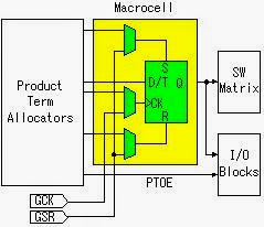
Fig.6 Block diagram of a macrocell inside CPLD
There are 18 independent macrocells in a function block, each macrocell is connected to the FastCONNECT Switch Matrix and I/O blocks. Moreover, PTOE (Product Term Output Enable) signal from Product Term Allocators is inputted into the I/O blocks. Since limitation of the number of the pins, it is not sometimes possible to use all macrocells.
System Programming of CPLD
XC9500 series of CPLD devices are programmed in-system via standard 4-pins JTAG (Joint Test Action Group) protocol and the devices fully support IEEE 11 49.1 boundary-scan (JTAG). Because of its equipped with the pin for independent JTAG, the program can be changed as it is mounted CPLD on the printed board.
While doing programming, all input ports in the I/O block are set to 'H' level. There are 4 wires used in JTAG as shown in Figure 7.

Fig.7 Block diagram of JTAG inside CPLD
More detail descriptions of these 4 wires of JTAG is as following:
- TMS (Test Mode Select)
- TCK (Test Clock)
- TDI (Test Data In)
- TDO (Read Data)
How to Program CPLD
The function of the CPLD device can be made using HDL (Hardware Description language) such as Verilog, VHDL, or ABEL. In order to write the file (JEDEC file) made using a fitting tool at the CPLD device, connection cable is needed.
The CPLD device from Xilinx Inc. is able to write data on the personal computer into the CPLD device using the JTAC protocol specified by IEEE 11 49.1 (JTAC boundary scan). Since the JTAG cable pins of XC9500 series consist of TMS, TCK, TDI and TDO, the data of the CPLD that is mounted on the printed board can be rewritten.

Fig.8 CPLD programming method (Xilinx Inc)
CPLD programming method based on Xilinx.Inc tool, a download cable is used to connect between a PC and a CPLD device. The cable is connected to the printer port (parallel port) of a PC using DSUB-25 connector.
Refereneces:
- http://www.xilinx.com/cpld
- .etc
No comments:
Post a Comment