Functional verification of hardware is used to verify functionality of the designed circuit. However, logic gates in real hardware have delays associated with the logic elements and paths inside. Therefore, we must also check whether the circuit design meets the timing requirements, the delay specifications for the logic designs. Checking timing requirements has become increasingly important as circuits have become smaller and faster.
One of the beauty of Verilog is allowing the Verilog user to specify delays (Gate and pin-to-pin delays) through the logic circuits. One of the ways to check timing is to do a timing simulation
that accounts for the delays associated with the block during the simulation.
Techniques other than timing simulation to verify timing have also emerged in the design automation industry. The most popular technique is static timing verification. Hardware designers first do a pure functional verification and then verify timing separately with a static timing timing verification tool. The main advantage of static verification is that it can verify timing in orders of magnitude more quickly than timing simulation. Static timing verification is a separate field of study and is not discussed in this discussion. We will discuss in detail how timing and delays are controlled and specified in Verilog modules. Thus, by using timing simulation, hardware designer can verify both functionality and timing of the circuit with Verilog.
Types of Delay Models
There are three types of delay models used in Verilog: distributed, lumped, and pin-to-pin (path) delays.
1. Distributed Delay
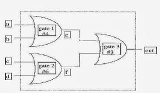
Distributed delay are specified on a per element basis. Delay values are assigned to individual elements in the circuit. An example of distributed delays is shown in the following figure.
Techniques other than timing simulation to verify timing have also emerged in the design automation industry. The most popular technique is static timing verification. Hardware designers first do a pure functional verification and then verify timing separately with a static timing timing verification tool. The main advantage of static verification is that it can verify timing in orders of magnitude more quickly than timing simulation. Static timing verification is a separate field of study and is not discussed in this discussion. We will discuss in detail how timing and delays are controlled and specified in Verilog modules. Thus, by using timing simulation, hardware designer can verify both functionality and timing of the circuit with Verilog.
Types of Delay Models
There are three types of delay models used in Verilog: distributed, lumped, and pin-to-pin (path) delays.
1. Distributed Delay
Distributed delay are specified on a per element basis. Delay values are assigned to individual elements in the circuit. An example of distributed delays is shown in the following figure.
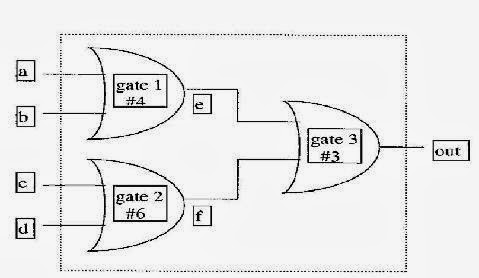
Distributed delay can be modeled by assigning delay values to individual gates or by using delay values in individual assign statements. When inputs of any gate change, the output of the gate changes after the delay value specified. Suppose the circuit above is named as module delay_OR, and the following example shows us how distributed delays are specified in gates and dataflow description.
Distributed delays in gate-level modules
//Distributed delay in each expression
assign #4 e = a & b;
assign #6 f = c & d;
assign #3 out = e & f;
Distributed delays provide detailed delay modeling. Delays in each element of the circuit are specified.
2. Lumped Delay
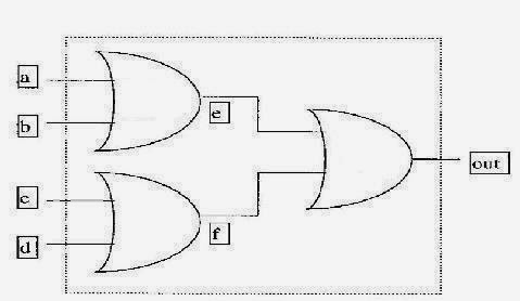
Lumped delay are specified on a per module basis. They can be specified as a single delay on the output gate of the module. The cumulative delay of all paths is lumped at one location. An example below shows a lumped delay.

In this example, maximum delay from any input to the output of the module delay_OR is computed, which is 6 + 3 = 9 units. The entire delay is lumped into the output gate. After a delay, primary output changes after any input to the module delay_OR changes.
Lumped delay in gate-level modules
Lumped delay models is easy to model compared with distributed delay.
2. Pin-to-Pin Delays
Another method of delay specification for a module is pin-to-pin timing delay. Delay are assigned individually to paths from each input to each output. Thus, delays can be separately specified for each input/output path. Figure below shows an example to compute the pin-to-pin delays for each input/output path.

Pin-to-pin delay for standard parts can be directly obtained from data books. Pin-to-pin delays for modules of a digital circuit are obtained by circuit characterization, using a low-level simulator like SPICE.
Although pin-to-pin delays are very detailed, for large circuits they are easier to model than distributed delays because the designer writing delay models needs to know only the I/O pins of the module rather than the internals of the module. The internals of the module may be designed by using gates, data flow, behavioral statements, or mixed design, but pin-to-pin delay specification remains the same. Pin-to-pin delays are also known as path delays. Topic on path delays in detail will be discussed in the next section path delay modeling.
To download sourcecode click below
----------------------------------------------------------------------------
module delay_OR (out, a, b, c, d); // declare parameters, variables
input a, b, c, d; // input variables
output out; // output variables
wire e, f;
//Delay is distributed to each gate
//Delay is distributed to each gate
and #4 a1(e, a, b);
and #6 a2(f, c, d);
and #3 a3(out, e, f);
//Distributed delay in data flow definition of a module
module delay_OR (out, a, b, c, d);
output out;
input a, b, c, d;
and #6 a2(f, c, d);
and #3 a3(out, e, f);
//Distributed delay in data flow definition of a module
module delay_OR (out, a, b, c, d);
output out;
input a, b, c, d;
wire e, f;
//Distributed delay in each expression
assign #4 e = a & b;
assign #6 f = c & d;
assign #3 out = e & f;
endmodule
---------------------------------------------------------------------------- Distributed delays provide detailed delay modeling. Delays in each element of the circuit are specified.
2. Lumped Delay
Lumped delay are specified on a per module basis. They can be specified as a single delay on the output gate of the module. The cumulative delay of all paths is lumped at one location. An example below shows a lumped delay.

In this example, maximum delay from any input to the output of the module delay_OR is computed, which is 6 + 3 = 9 units. The entire delay is lumped into the output gate. After a delay, primary output changes after any input to the module delay_OR changes.
Lumped delay in gate-level modules
----------------------------------------------------------------------------
//Lumped Delay Model
module delay_OR (out, a, b, c, d); // declare parameters, variables
input a, b, c, d; // input variables
input a, b, c, d; // input variables
output out; // output variables
wire e, f;
and a1(e, a, b);
and a2(f, c, d);
and #9 a3(out, e, f); // delay only on the output gate
and a2(f, c, d);
and #9 a3(out, e, f); // delay only on the output gate
endmodule
---------------------------------------------------------------------------- Lumped delay models is easy to model compared with distributed delay.
2. Pin-to-Pin Delays
Another method of delay specification for a module is pin-to-pin timing delay. Delay are assigned individually to paths from each input to each output. Thus, delays can be separately specified for each input/output path. Figure below shows an example to compute the pin-to-pin delays for each input/output path.
path a-e-out, delay = 7
path b-e-out, delay = 7
path c-f-out, delay = 9
path d-f-out, delay = 9
Pin-to-pin delay for standard parts can be directly obtained from data books. Pin-to-pin delays for modules of a digital circuit are obtained by circuit characterization, using a low-level simulator like SPICE.
Although pin-to-pin delays are very detailed, for large circuits they are easier to model than distributed delays because the designer writing delay models needs to know only the I/O pins of the module rather than the internals of the module. The internals of the module may be designed by using gates, data flow, behavioral statements, or mixed design, but pin-to-pin delay specification remains the same. Pin-to-pin delays are also known as path delays. Topic on path delays in detail will be discussed in the next section path delay modeling.
Reference:
- Verilog HDL, A guide to Digital Design and Synthesis, 2nd edtion, Samir Palnitkar, SunSoft Press - A Prentice Hall Title.
To download sourcecode click below
No comments:
Post a Comment